Showing posts with label ANALOG ELECTRONICS-7BPH5C1-2019-ODD SEM. Show all posts
Showing posts with label ANALOG ELECTRONICS-7BPH5C1-2019-ODD SEM. Show all posts
III Internal Test - Analog Electronics -7BPH5C1
Analog Electronics - 7BPH5C1
III Internal Test
Time : 2 Hrs Marks: 40
PART - A 5 x 2 = 10
1.What is negative feedback?
2. State Barhausen Criterion.
3.Define Bandwidth.
4.Write note on collector efficiency.
5.Draw the symbol of an Op-Amp.
PART - B 2 x 5 = 10
2.List the differences between voltage and power amplifiers.
3.List the Characteristics of an Ideal Op-Amp
4.Explain the working of an Op-Amp as an integrator
PART - C 2 x 10 = 20
2.With neat diagram explain the working of Hartley Oscillator.
3.Discuss the working of Instrumentation Amplifier with appropriate diagram.
II Internal Test - Analog Electronics
Analog Electronics - 7BPH5C1
II Internal Test
Time : 2.5 Hrs Marks: 40
PART - A 5 x 2 = 10
1.What is Stability Factor? Give its importance.
2.Write note on Thermal Runaway.
3.Define Input Impedance of a CE Amplifier
4.Write an Expression for Power Dissipation in a CE Amplifier
5.Define CMRR
PART - B 2 x 5 = 10
2.Write note on Cut Off and Saturation Points.
3.Draw the DC Equivalent Circuit of Single Stage CE Amplifier and Explain its function.
4.Compare different types of Coupling Schemes for Multistage Amplifier.
PART - C 2 x 10 = 20
2.Describe the working of inverting and non-inverting amplifiers using op-amps.
3.Discuss the working of Op-Amp Differentiator and Adder circuits.
Short Q & A For the I Internal Test
1.What are extrinsic semiconductors?
An Extrinsic Semiconductor is a semiconductor material doped by a specific impurity, which is able to modify its electrical properties,making it suitable for electronic applications with specific purposes. An extrinsic semiconductor may be of P type with holes as majority charge carriers or of N type with electrons as majority charge carriers.
2. What is a Crystal Diode?
A crystal diode is made by making a cat whisker metal wire tip in contact with a silicon or germanium crystal under pressure. During the manufacture of the point contact diode, a relatively large current is passed from the cat whisker to the silicon crystal. The result of this large current is the formation of a small region of p-type material around the crystal in the vicinity of the point contact.Thus, a PN-junction is formed which behaves in the same ways a normal PN-junction.3.
3. Define Ripple Factor
Ripple factor of a rectifier is defined as the ratio of the root mean square value of AC component of the output to the average DC component of the output.
4. Define Current Gain of a CC Amplifier
Common collector current gain is defined as the ratio between emitter current and base current in common collector configuration.
Viz.,
5. Define Operating Point of a Transistor
The operating point of a transistor, also known as bias point, quiescent point, Q-point, is the steady-state (DC) voltage or current at a specified terminal of the transistor with no input signal applied.
I Internal Test - Analog Electronics
Analog Electronics - 7BPH5C1
I Internal Test
Time : 2.5 Hrs Marks: 60
PART - A 5 x 2 = 10
1.What are extrinsic semiconductors?
2.What is a crystal diode?
3.Define ripple factor.
4.Define current gain of a transistor in CC mode.
5.Define operating point of a transistor.
PART - B 4 x 5 = 20
2. Derive relation between alpha and beta.
3. Compare the characteristics of transistors connected in CB,CE and CC mode.
4. Compare different types of coupling in multistage amplifier.
PART - C 3 x 10 =30
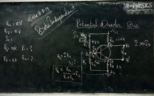
2.Explain the Voltage Divider Bias method for biasing a transistor.
3.Describe the working of a single stage CE amplifier with a neat diagram.
Fixed Base Bias - Unruly Behavior at a High β Value Vs Feedback Resistor Bias For the Same β - No Clipping and Harmonics
Click This LINK to Interact with the Simulation of Fixed Base Bias - CE Amplifier. Note that negative half cycles are nearly cut-off at the output. Also look at the presence of harmonics in the output's frequency spectrum.
Click This LINK to Interact with the Simulation of Feedback Resistor Bias - CE Amplifier.No clipping, distortion and the presence of harmonics in the output's frequency spectrum though the gain has been sacrificed a bit.
Click This LINK to Interact with the Simulation of Feedback Resistor Bias - CE Amplifier.No clipping, distortion and the presence of harmonics in the output's frequency spectrum though the gain has been sacrificed a bit.
ATTENTION: Assignment I - Fixed Base Bias - FINAL DATE: 14.08.2019 Wednesday
Assuming the Set of Collector Curves provided below for the above CE Amplifier Circuit and taking VCC = 12 V and β = 50
(i) Design the Circuit( Viz., Find the Component Values).
(ii) Draw the load line and note the Quiescent Point on it.
(iii) Now assume β = 100. For the same Component Values draw the load line and note the Quiescent Point again on the load line.
(iv) What is the big difference?
A Fly flied in and An Elephant came out - Don't You Believe Me?
Here is snapshot of the picture I mentioned during my lecture from the Book : Entertaining Electronics by E.Sedov. Click HERE to download the book.
When I was a small boy I read this book in Tamil and immensely enthused by it in the field of electronics. I can never forget those days of adventures in happy reading.
Ultragel - Removing the Acoustic Impedance Mismatch Between The Transducer and The Human Body
Here is Steve Mould's Video On the Topic :
Comparison of Transistor Configurations
|
TRANSISTOR
CONFIGURATION
|
COMMON
BASE
|
COMMON
EMITTER
|
COMMON
COLLECTOR
|
|
|
|
|
|
|
VOLTAGE GAIN
|
High
|
Medium
|
Low(Nearly
Unity)
|
|
|
|
|
|
|
CURRENT GAIN
|
Low
(Nearly Unity)
|
Medium
|
High
|
|
|
|
|
|
|
POWER GAIN
|
Low
|
High
|
Medium
|
|
|
|
|
|
|
INPUT/OUTPUT PHASE RELATION
|
0°
|
180°
|
0°
|
|
|
|
|
|
|
INPUT IMPEDANCE
|
Low
|
Medium
|
High
|
|
|
|
|
|
|
OUTPUT IMPEDANCE
|
High
|
Medium
|
Low
|
|
|
|
|
|
|
APPLICATIONS
|
Pre-amplifiers
VHF
and UHF Amplifiers
Current
Buffers
Impedance
Matching
|
LF
and RF Amplifiers
Electronic
Switches
Oscillators
|
Impedance
Matching
Voltage
Buffers
Driver
Amplifiers
|
Subscribe to:
Posts (Atom)


