Click HERE to download as a PDF
CCD Operation
A Charge Coupled Device (CCD) is
a highly sensitive photon detector. The CCD is divided up into a large number
of light-sensitive small areas (known as pixels) which can be used to build up
an image of a scene. A photon of light which falls within the area defined by
one of the pixels will be converted into one (or more) electrons and the number
of electrons collected will be directly proportional to the intensity of the
scene at each pixel. When the CCD is clocked out, the number of electrons in
each pixel is measured and the scene can be reconstructed.
The figure below shows a
simplified cross section through a CCD. The pixels are defined by the position
of electrodes above the CCD. If a positive voltage is applied to the electrode,
then this positive potential will attract all of the negatively charged
electrons close to the area under the electrode. In addition, any positively
charged holes will be repulsed from the area around the electrode. Consequently
a potential well will form in which the electrons produced by the incoming
photons will be stored.
As more and more light falls
onto the CCD, then the potential well surrounding this electrode will attract
more and more electrons until the potential well is full. To prevent this
happening the light must be prevented from falling onto the CCD for example, by
using a shutter as in a camera. Thus, an image can be made of an object by
opening the shutter, "integrating" for a length of time to fill up
most of the electrons in the potential well, and then closing the shutter to
ensure that the full well capacity is not exceeded.
An actual CCD will consist of a large number
of pixels (i.e., potential wells), arranged horizontally in rows and vertically
in columns. The number of rows and columns defines the CCD size, typical sizes
are 1024 pixels high by 1024 pixels wide. The resolution of the CCD is defined
by the size of the pixels, also by their separation (the pixel pitch).
CCD Operation
The figure below shows a cross
section through a row of a CCD. Each pixel consists of three electrodes IØ1,
IØ2, and IØ3. Only one of these electrodes is required to create the potential
well, but other electrodes are required to transfer the charge out of the CCD.
The upper section of the figure (section 1) shows charge being collected under
one of the electrodes. To transfer the charge out of the CCD, a new potential
well can be created by holding IØ3 high, the charge is now shared between IØ2
and IØ3 (section 2). If IØ2 is now taken low, the charge will be fully
transferred under electrode IØ3 (section 3). To continue clocking out the CCD,
taking IØ1 high and then taking IØ3 low will ensure that the charge cloud now
drifts across under the IØ1 electrodes. As this process is continued, the
charge cloud will progress either down the column, or across the row, depending
upon the orientation of the electrodes.
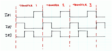
The figure below (clocking diagram) shows the progression under which each electrode is held high
and low to ensure that charge is transferred through the CCD.
Initially, IØ2 is high - usually
to around 12V, and the charge is held under that electrode as in (1)
previously. When IØ3 is held high, and IØ2 is taken low (usually 0 V), the
charge migrates under the IØ3 electrode (as in (2)). Finally, taking IØ1 high
and IØ3 low transfers the charge under IØ1 (as in (3)). This process is
repeated in transfer 2 and transfer 3, the charge has now been moved three
pixels along. This process is known as charge coupling (hence CCD).
For most of the CCD, the
electrodes in each pixel are arranged so that the charge is transferred
downwards along the columns. Hence, during the CCD clocking operation, rows are
transferred downwards to the final row (the readout register) which is used to
transfer the charge in each pixel out of the CCD so it can be measured.
In the read out register, the
electrodes are arranged so that the charge is transferred in the horizontal
direction, along the readout register.
The final process on the CCD is
the reading of each pixel so that the size of the associated charge cloud can
be measured. At the end of the readout register is an amplifier which measures
the value of each charge cloud and converts it into a voltage.


